
As semiconductor roadmaps grow more complex and traditional scaling approaches encounter diminishing returns, a new generation of innovation is emerging from two unexpected but increasingly influential corners: quantum technologies and Micro-electromechanical Systems (MEMS). These once-specialized domains are drawing fresh interest, not only from startups and researchers but also from seasoned veterans in the industry. Erik Hosler, a seasoned advisor and technical strategist in advanced lithography and patterning, highlights this convergence as part of a broader effort to diversify problem-solving approaches at a system level.
It is not merely a trend born of hype. Industry veterans have a long history of discerning between speculative technologies and those that represent actionable engineering pathways. What they see now in both quantum and MEMS is a unique confluence of maturity, cross-domain potential, and critical relevance to emerging challenges in semiconductor design, inspection, and integration. As tools, materials, and architectures develop, both domains are positioned not at the periphery but as integral components of the future chipmaking stack.
Beyond the Node Race: New Priorities for Innovation
The traditional driver of semiconductor progress, shrinking the process node, has reached a stage where returns are neither guaranteed nor uniform. While EUV has extended Moore’s Law into the 3-nanometer class and beyond, the cost, stochastic variation, and integration complexity have made continued scaling increasingly selective.
That has caused a strategic shift. More engineers and executives are now asking what else can be optimized beyond just feature size. That question has opened the door to technologies that were once considered niche or adjunct, like quantum devices for computing and sensing and MEMS for integration, packaging, and signal processing.
What draws attention to both domains is not just their functionality but their capacity to interface with other parts of the semiconductor stack. MEMS, for example, are no longer confined to accelerometers and microphones. It is playing a growing role in optics, thermal regulation, and chip-to-chip alignment. Similarly, quantum circuits, though in the initial stages, are shaping how companies think about low-power logic, cryptography, and high-throughput sensing.
The MEMS Advantage: Small Scale, Big Versatility
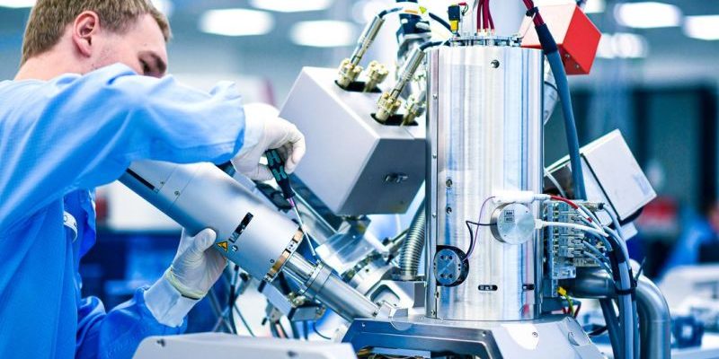
MEMS devices are built using many of the same fabrication methods as ICs, but they bring quite a separate set of capabilities. These mechanical systems, often based on silicon substrates, can move, bend, resonate, and detect with extreme precision. That makes them well-suited for a variety of next-generation applications, from nano-positioning in lithography tools to tunable RF components and even packaging innovations in 3D chip stacks.
Veteran engineers have noted MEMS’ ability to operate hybrid systems. Unlike pure digital solutions, MEMS-based mechanisms can provide analog responses, feedback control, and physical interaction with the environment. As chip architectures develop to include more layers, optical interconnects, and heterogeneous integration, MEMS plays a crucial enabling role.
The infrastructure for MEMS development has also matured. Foundries, simulation tools, and material platforms now exist that allow MEMS to be prototyped and productized with increasing efficiency. It lowers the barrier to entry and allows more exploratory designs to reach commercial feasibility, a crucial factor when seasoned engineers look for stability in emerging tech bets.
Quantum Interest: Early, Yet Essential
Quantum technology represents different kinds of challenges and opportunities. While much of the attention is on quantum computing, its implications for semiconductor technology are broader and potentially deeper. Quantum sensors, for instance, offer performance metrics far beyond classical devices in fields such as magnetic imaging, timing, and even semiconductor defect detection.
Stakeholders are particularly interested in how quantum effects may reshape device physics and inspection methods. As process nodes shrink and metrology becomes harder, quantum-driven tools can offer new levels of resolution and precision. Certain materials being explored for quantum devices, such as topological insulators and Josephson junctions, may also influence material innovation across classical components.
This convergence of material research, architectural design, and exploratory physics has started to appeal to engineers who remember earlier inflection points, such as the shift to FinFETs or the adoption of EUV. Quantum may not yet be ready to scale commercially, but its foundational research is producing spinoffs that are immediately relevant to conventional semiconductor workflows.
Panel Discussions as Innovation Beacons
One of the clearest indications of the growing seriousness with which these technologies are taken is their presence in high-level panel discussions. No longer treated as speculative detours, MEMS and quantum systems are being discussed as integral parts of the roadmap.
At the SPIE lithography conference, industry leaders across domains, from patterning specialists to materials experts, gathered to exchange insights on how these technologies intersect with core lithographic and metrological challenges. Panel sessions are no longer siloed by discipline. They are engineered for convergence.
Erik Hosler remarks, “We are looking at just about everything in advanced patterning.” This inclusive lens suggests that traditional lithography is being expanded to include influences from mechanical systems, quantum behavior, and cross-domain modeling. The goal is not just to refine techniques but to reframe the boundaries of what advanced patterning encompasses.
The Veteran Perspective: Pattern Recognition and Long Horizons
Industry veterans bring something essential to the table: pattern recognition. Many have seen the rise and fall of countless technologies, but they’ve also witnessed how underestimated ideas, like immersion lithography or chip stacking, can become central pillars of future systems.
Their renewed focus on quantum and MEMS isn’t purely theoretical. It’s informed by what these technologies are already doing in labs, pilot programs, and hybrid architectures. These engineers understand that long-term bets require near-term footholds. Increasingly, both MEMS and quantum research produce usable tools, inspection methods, and design inspirations that feed directly into commercial development. What stands out is how many of these veterans are joining advisory boards, research alliances, or launching targeted initiatives focused on these areas. Their engagement isn’t abstract. It’s hands-on.
From Curiosity to Strategy
What started as a curiosity-driven expansion of the roadmap is now becoming strategic. Companies are allocating real budgets, time, and talent to MEMS and quantum initiatives. Research consortia formalize relationships between quantum physicists and lithographers, while MEMS designers collaborate with packaging teams to co-optimize mechanical stability and thermal performance.
That is where the convergence deepens. MEMS actuators can align optical components for quantum processors, and quantum sensors can detect irregularities in MEMS device behavior. The boundary between the two domains begins to blur, yielding systems that are more integrated, more robust, and more adaptable. Veteran voices are helping to guide this integration with realism. They push for proof points, cost models, and manufacturability metrics. But they also advocate patience, encouraging teams not to shy away from these emerging areas simply because timelines are uncertain.


Comments